Overview
As the global artificial intelligence compute buildout transitions from training dense foundation models toward trillion-parameter real-time inference clusters, the competitive landscape across the High Bandwidth Memory sector is undergoing a generational shift. Semiconductor leader
Nvidia has established the upcoming HBM4 memory architecture as the foundational component powering its next-generation Rubin computing platform. At this technological inflection point,
Nasdaq listed
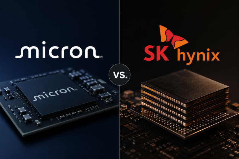
Micron Technology and
Korea Exchange market leader
SK Hynix are locked in an intensive struggle for market dominance. According to research published by
Reuters, the HBM4 specification represents an architectural departure from prior generations, doubling the physical interface bus from 1024 bits to 2048 bits while requiring the base logic die to be manufactured on advanced pure-play foundry nodes rather than traditional memory processes. This paradigm shift reshapes thermal and electrical integration between memory stacks and accelerator silicon, creating a high-stakes operational contest across fabrication yields, advanced packaging integration, and geographic supply chain resiliency.
Key Takeaways
Structural architectural transformation redefines memory manufacturing as HBM4 introduces a 2048-bit interface and transitions base logic die fabrication to advanced foundry processes, transforming High Bandwidth Memory from standardized commodity silicon into customized system-on-chip assemblies.
SK Hynix leverages established packaging moats and alliance integration, utilizing proprietary Mass Reflow Molded Underfill technology alongside a tripartite engineering alliance with
TSMC and Nvidia to maintain incumbent delivery leadership.
Micron Technology executes an aggressive node offensive via 1-beta DRAM architecture, delivering structural energy efficiency and density advantages while leveraging domestic United States manufacturing expansion and federal subsidies to capture long-term enterprise allocation.
Multi-billion-dollar capital expenditure budgets pressure operational cash flows, as 16-high die stacking and transition timelines toward hybrid bonding require massive cleanroom investments while companies strive to defend gross margins above the 70% threshold.
Dynamic dual-sourcing procurement frameworks govern enterprise allocation, with Nvidia deploying competitive multi-vendor allocations across the Rubin platform to mitigate single-supplier supply shocks and optimize procurement expenses.
The Architectural Paradigm Shift in HBM4: Custom Base Dies and 2048-Bit Interfaces
Throughout prior memory cycles, transitions from HBM2E to HBM3 and HBM3E relied primarily on incremental DRAM die shrinks and clock frequency optimizations. The transition to HBM4 breaks this historical progression through structural physical redesign.
Transitioning from Standard Memory to Advanced Foundry Logic Integration
Analysis published by
Bloomberg indicates that the most consequential engineering innovation within HBM4 is shifting base die fabrication to external foundry lines. In preceding generations, the base die was manufactured internally by memory fabricators using mature DRAM processes. Under HBM4 specifications, routing 2048 high-speed physical channels directly to host graphics processors requires base dies to be fabricated on 5-nanometer or 3-nanometer logic nodes. This structural requirement forces memory makers to integrate their proprietary memory stacks directly into TSMC advanced packaging ecosystems, replacing independent memory supply models with co-engineered foundry integrations.
Sixteen-Layer Stacking and Thermal Dissipation Challenges
To eliminate memory bandwidth bottlenecks during multi-modal inference, HBM4 doubles the bus interface to 2048 bits, pushing peak theoretical throughput beyond 1.5 terabytes per second per stack. Concurrently, vertical die stacking expands from 8-high and 12-high configurations toward 16-high assemblies. Industry disclosures reviewed by the
Financial Times confirm that 16-high stacking requires individual DRAM wafers to be ground down to micro-level thickness. Managing wafer warpage, micro-bump solder bridging, and thermal hotspots under continuous high-power compute workloads represents the primary technical barrier separating tier-one fabricators.
SK Hynix Incumbent Leadership: MR-MUF Packaging and Proven Nvidia Integration
As the primary incumbent supplying High Bandwidth Memory for Nvidia flagship computing architectures, SK Hynix maintains substantial structural advantages entering the HBM4 generation.
Thermal Management Moats and Packaging Yield Superiority
SK Hynix established market leadership through its proprietary Mass Reflow Molded Underfill (MR-MUF) packaging technology. By injecting liquid epoxy molding compound between micro-bumps and applying uniform thermal pressure, the process minimizes internal voids while improving thermal conductivity relative to standard non-conductive film alternatives. For 16-high HBM4 configurations, SK Hynix has advanced its proprietary packaging process to preserve structural stability and maintain industry-leading assembly yields.
The Tripartite Alliance with TSMC and Nvidia
Addressing customized base logic die integration, SK Hynix executed direct technical collaboration agreements with TSMC. By pre-testing its memory stacking architectures with TSMC CoWoS advanced packaging flows, SK Hynix, TSMC, and Nvidia operate a closed engineering feedback loop. Financial disclosures submitted to the
U.S. Securities and Exchange Commission highlight that this structured alignment reduces sample qualification cycles, giving SK Hynix an operational head start in delivering initial engineering samples for Nvidia Rubin compute platforms.
Micron 1-Beta Node Offensive: Density Advantages and Onshoring Premiums
While Micron entered the commercial High Bandwidth Memory market later than its primary competitor, the North American semiconductor fabricator is utilizing advanced material science and aggressive node transitions to challenge incumbent market share.
Energy Efficiency Breakthroughs via Advanced Node Skipping
Micron's strategic positioning centers on skipping intermediate development steps to focus resources directly on the 1-beta DRAM node. Utilizing multi-patterning immersion lithography without early reliance on EUV tooling for critical layers, Micron achieved high transistor density alongside a 25% reduction in module power consumption compared to competing solutions. In multi-megawatt data centers where electrical power availability limits computational density, Micron's lower thermal footprint provides tangible total cost of ownership advantages during hyperscaler procurement negotiations.
Geopolitical Diversification and North American Manufacturing Subsidies
Reporting from
The Wall Street Journal underscores that leading compute designers are prioritizing geographic supply chain diversification to mitigate regional disruption risks. Backed by federal grants under the CHIPS and Science Act, Micron is expanding advanced fabrication and packaging facilities across New York and Idaho. This domestic manufacturing footprint provides enterprise clients with onshore delivery capabilities, establishing a resilient non-tariff competitive advantage when competing for long-term Rubin platform procurement allocations.
Market participants actively trading technology breakouts and managing volatility can utilize specialized derivatives tools on institutional platforms.
Furthermore, order book metrics on
MEXC demonstrate sustained depth and cross-market turnover across major equities-linked digital assets during major technological transitions.
Capital Allocation and Operating Leverage: CapEx Durability vs Gross Margin Resiliency
Evaluating the long-term investment case for Micron and SK Hynix requires assessing cash flow conversion efficiency alongside balance sheet durability.
Operating Profitability Tied to Custom Memory Pricing Power
Quarterly financial disclosures confirm that High Bandwidth Memory products generate exceptional profitability, sustaining gross margins between 60% and 75%, significantly outperforming standard commodity DRAM. However, incorporating external advanced foundry logic dies from TSMC alongside advanced testing regimes elevates input bill of materials costs for HBM4. The manufacturer that sustains superior packaging yields will better absorb external foundry fees, preserving higher free cash flow conversion rates over upcoming reporting periods.
Megafab Outlays Across Yongin and New York Infrastructure Projects
Advanced memory fabrication represents a capital-intensive manufacturing cycle. SK Hynix is deploying tens of billions of dollars into its Yongin semiconductor mega-cluster, while Micron is matching these capital expenditures across domestic megafab projects. Commentary from
CNBC highlights that procuring advanced lithography tools, deep silicon via etching equipment, and thermo-compression bonders requires massive cash flow commitments. If deployment schedules for next-generation AI server architectures experience temporary delivery pauses, fixed asset depreciation could create cyclical pressure on operating margins.
Nvidia Rubin Allocation Strategy and Critical Forward Indicators
Nvidia procurement framework for the Rubin architecture serves as the primary external determinant of market share distribution and relative equity valuations.
In commercial practice, enterprise compute designers avoid single-source supplier concentration. By splitting procurement allocations across SK Hynix, Micron, and
Samsung Electronics, Nvidia protects its operational resilience while maintaining pricing leverage over upstream hardware components.
Market participants analyzing the competitive trajectory of both companies should monitor several key operational checkpoints:
Initial sample validation metrics on the Nvidia Rubin computing platform, focusing on real-world thermal resistance, signal eye diagrams, and sustained 2048-bit bus bandwidth.
TSMC monthly advanced logic base die and CoWoS packaging allocation distribution, verifying whether external foundry capacity limits shipment run-rates for either supplier.
Sixteen-layer stacking yield progress, tracking when commercial volume production yields reliably cross the eighty percent profitability threshold.
Exclusive View from James Mitchell
From a quantitative market structure and semiconductor cycle perspective, the HBM4 battle between Micron and SK Hynix marks the definitive transformation of High Bandwidth Memory from a cyclical memory commodity into high-margin specialized system architecture.
Market participants frequently make the mistake of assuming that SK Hynix incumbent market share from the HBM3E cycle will transfer automatically into the HBM4 generation. Quantitative derivatives skew and institutional order flow indicate that capital is actively pricing in Micron competitive potential. The requirement for advanced TSMC logic base dies effectively resets the manufacturing baseline, requiring all fabricators to optimize assembly flows within a collaborative tripartite structure. Micron 1-beta architecture delivers power efficiency that directly addresses data center thermal constraints where rack power density approaches substation thresholds. For professional market participants, the critical forward indicator is not headline marketing announcements, but the confirmed supplier allocation percentages in Nvidia definitive procurement agreements alongside the durability of gross margin guidance across subsequent quarterly earnings reports.
FAQ
What is HBM4 and how does it differ from HBM3E?
HBM4 is the next-generation High Bandwidth Memory standard. It doubles the physical bus interface from 1024 bits to 2048 bits to increase data throughput, and transitions base logic die fabrication to advanced logic foundry processes like TSMC, transforming memory modules into customized system-on-chip assemblies.
Why is the Nvidia Rubin architecture dependent on HBM4 memory?
Nvidia next-generation Rubin computing platform is engineered for multi-trillion parameter artificial intelligence inference and mixture-of-experts architectures, demanding extreme data bandwidth. HBM4 provides the necessary data throughput and power efficiency to prevent compute cores from idling while waiting for memory retrieval.
What are SK Hynix primary competitive advantages in HBM4?
SK Hynix commands deep engineering moats in Mass Reflow Molded Underfill packaging, delivering proven thermal dissipation and high assembly yields across dense vertical stacks. Additionally, its established tripartite engineering alliance with TSMC and Nvidia provides early sample qualification advantages.
How is Micron Technology challenging SK Hynix leadership?
Micron advanced directly to the 1-beta manufacturing node, achieving high transistor density and reducing memory power consumption by approximately 25%. Furthermore, Micron domestic United States manufacturing investments and federal grant backing provide critical supply chain diversification for North American customers.
What role does TSMC play in the HBM4 competition?
TSMC operates as the central manufacturing hub for HBM4. Because HBM4 base logic dies require advanced 5nm or 3nm logic nodes and must be integrated alongside compute silicon using CoWoS packaging, TSMC foundry capacity and packaging allocations directly influence production timelines for both memory makers.
What key milestones should investors monitor to determine the market leader?
Investors should track engineering sample performance metrics on Nvidia Rubin test platforms, official supplier allocation percentages, 16-high stacking volume manufacturing yields, and quarterly gross margin trends for specialized memory product lines.
Disclaimer
The information, analysis, and views contained in this article are provided for general educational and informational purposes only and do not constitute financial advice, investment advice, legal advice, tax advice, or a recommendation to buy or sell any security, digital asset, or financial derivative. Equity securities and financial instruments are subject to high market volatility and capital risk. Past operational performance, financial results, and quantitative indicators do not guarantee future market returns. Investors must conduct independent due diligence and evaluate their personal financial situation, risk tolerance, and investment goals before executing any trade. The MEXC Crypto Pulse team assumes no liability for any direct or indirect financial losses resulting from the use of or reliance upon the information published herein.
About the Author
James Mitchell specializes in technical analysis, market trends, and trading strategies for both Bitcoin and altcoins. Based in London, he has over 10 years of experience in financial markets. Before joining MEXC Learn, James worked as a senior analyst at a leading European investment firm, where he developed expertise in risk management and quantitative trading. His transition to cryptocurrency markets began in 2017, and he has since become recognized for his data-driven approach. He holds a Master's degree in Financial Economics from the London School of Economics. His analytical approach combines traditional technical analysis with on-chain metrics to provide readers with actionable insights. Areas of expertise include technical analysis, market trends and cycles, trading strategies, Bitcoin and altcoin analysis, and risk management.
Research References